QuadLock: Difference between revisions
Jump to navigation
Jump to search
No edit summary |
|||
| Line 5: | Line 5: | ||
=== Blocks === | === Blocks === | ||
==== Block A ==== | |||
Internal amplifier 4 channels | |||
pin 1: Speaker Rear Right, positive | |||
pin 2: Speaker Front Right, positive | |||
pin 3: Speaker Front Left, positive | |||
pin 4: Speaker Rear Left, positive | |||
pin 5: Speaker Rear Right, negative | |||
pin 6: Speaker Front Right, negative | |||
pin 7: Speaker Front Left, negative | |||
pin 8: Speaker Rear Left, negative | |||
==== Block B ==== | |||
Microphones, [[FBAS]], debug, hands-free kit | |||
pin 01: Microphone 1, positive | |||
pin 02: Microphone 2, negative | |||
pin 03: j5 debug terminal, RX | |||
pin 04: VDA NF, positive | |||
pin 05: VDA Mute | |||
pin 06: FBAS1 in, positive | |||
pin 07: Microphone 1, negative | |||
pin 08: Microphone 2, positive | |||
pin 09: j5 debug terminal, TX | |||
pin 10: VDA NF, negative | |||
pin 11: V850 debug terminal, TX | |||
pin 12: FBAS1 in, shield | |||
==== Block C ==== | |||
TODO | |||
==== Block D ==== | |||
TODO | |||
==== Block E ==== | |||
TODO | |||
=== Pinout === | === Pinout === | ||
Revision as of 00:06, 27 March 2025
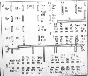
Main connector behind infotainment unit. Originally it featured 4 blocks of pins - hence the name. Since the original 1st generation of QuadLock, infotainment needs changed and the connector evolved. Basic shape stayed the same but block structure was adapted for newer system requirements.
QuadLock Gen3

Blocks
Block A
Internal amplifier 4 channels
pin 1: Speaker Rear Right, positive
pin 2: Speaker Front Right, positive
pin 3: Speaker Front Left, positive
pin 4: Speaker Rear Left, positive
pin 5: Speaker Rear Right, negative
pin 6: Speaker Front Right, negative
pin 7: Speaker Front Left, negative
pin 8: Speaker Rear Left, negative
Block B
Microphones, FBAS, debug, hands-free kit
pin 01: Microphone 1, positive
pin 02: Microphone 2, negative
pin 03: j5 debug terminal, RX
pin 04: VDA NF, positive
pin 05: VDA Mute
pin 06: FBAS1 in, positive
pin 07: Microphone 1, negative
pin 08: Microphone 2, positive
pin 09: j5 debug terminal, TX
pin 10: VDA NF, negative
pin 11: V850 debug terminal, TX
pin 12: FBAS1 in, shield
Block C
TODO
Block D
TODO
Block E
TODO
Pinout
//TODO → FBAS2 mode
Repair kit
//TODO